

DRAM ETF PCF Changes: The Sentiment Signal
Semiconductor ETFs are often viewed as simple vehicles for gaining diversified exposure to the chip industry. Yet beneath the familiar ETF price chart is a detailed portfolio construction process that can reveal useful information about market expectations. One particularly interesting source of information is the portfolio composition file, commonly referred to as the PCF. Changes in the PCF can show how an ETF's underlying basket is being adjusted, and for DRAM-related semiconductor strategies, these adjustments may provide an early indication of changing investor sentiment.

Electronic Grade NaOH: The Cleaning Process Purity Upgrade
In semiconductor materials, the most valuable upgrade is not always a new molecule. Sometimes it is a familiar chemical delivered with tighter impurity limits, cleaner packaging, better analytical verification, and more dependable batch consistency. Electronic-grade sodium hydroxide belongs to that category: a conventional alkaline chemical whose usefulness depends on the application and the contamination controls surrounding it.
CMP Consumables Business Model: The Recurring Revenue Advantage
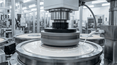
Chemical mechanical planarization has an attractive commercial characteristic: the equipment is purchased periodically, but the materials that make it productive are consumed repeatedly. Every qualified polishing process creates continuing demand for slurry, pads, conditioners, cleaning chemistry, and other supporting products.
Nvidia Rubin’s 288GB HBM4 Configuration: Memory Bandwidth as the New Compute Bottleneck
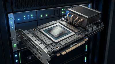
An AI accelerator can contain extraordinary arithmetic capability and still spend valuable time waiting for data. That gap between what a processor can calculate and what its memory system can supply is central to Nvidia’s Rubin architecture.

STOXX Europe Semi vs. US Semi: The Long-Term Return Attribution
Europe builds some of the semiconductor industry’s most difficult-to-replace technology. US-listed semiconductor companies include businesses that capture substantial value from chip architecture, computing platforms, and manufacturing equipment. Both belong to the same global production system, yet their equity benchmarks can follow very different paths.
Popular Articles
DRAM ETF PCF Changes: The Sentiment Signal
Semiconductor ETFs are often viewed as simple vehicles for gaining diversified exposure to the chip industry. Yet beneath the familiar ETF price chart is a detailed portfolio construction process that can reveal useful information about market expectations. One particularly interesting source of information is the portfolio composition file, commonly referred to as the PCF. Changes in the PCF can show how an ETF's underlying basket is being adjusted, and for DRAM-related semiconductor strategies, these adjustments may provide an early indication of changing investor sentiment.
HBM’s Crowding-Out Effect on DDR4 Supply: The Legacy Memory Shortage
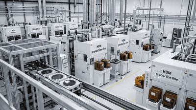
The memory market has developed an uncomfortable contradiction: the technology manufacturers are eager to leave behind can become the product customers struggle hardest to replace. DDR4 is no longer the preferred destination for much of the industry’s new investment, yet a substantial installed base still depends on it.
CMP Consumables Business Model: The Recurring Revenue Advantage
Chemical mechanical planarization has an attractive commercial characteristic: the equipment is purchased periodically, but the materials that make it productive are consumed repeatedly. Every qualified polishing process creates continuing demand for slurry, pads, conditioners, cleaning chemistry, and other supporting products.
Nvidia Rubin’s 288GB HBM4 Configuration: Memory Bandwidth as the New Compute Bottleneck
An AI accelerator can contain extraordinary arithmetic capability and still spend valuable time waiting for data. That gap between what a processor can calculate and what its memory system can supply is central to Nvidia’s Rubin architecture.
Intel’s Glass Substrate Pivot: A Foundry Comeback Strategy or a Packaging Play?
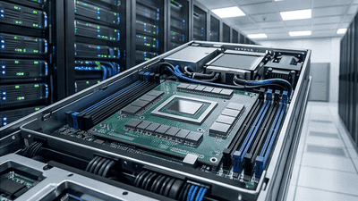
Intel’s glass-substrate strategy is primarily a packaging opportunity that could strengthen its foundry business—not a substitute for rebuilding competitive wafer manufacturing. That distinction matters because packaging can attract customers and improve system performance without automatically proving that Intel’s process technology, manufacturing economics, or external foundry model has recovered.
Macro Cycle
Intel’s Glass Substrate Pivot: A Foundry Comeback Strategy or a Packaging Play?
Intel’s glass-substrate strategy is primarily a packaging opportunity that could strengthen its foundry business—not a substitute for rebuilding competitive wafer manufacturing. That distinction matters because packaging can attract customers and improve system performance without automatically proving that Intel’s process technology, manufacturing economics, or external foundry model has recovered.

The $4 Trillion Data Center Buildout: Where Semiconductor Spending Concentrates
The semiconductor money in the data center build-out concentrates in four places: accelerated compute, high-performance memory, networking, and the manufacturing technologies needed to integrate them. Power management, storage, and host processors capture additional demand, but the spending is not distributed evenly across the chip industry.
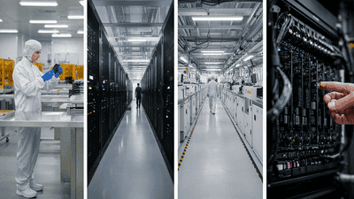
Why the Fed’s Rate Hike Didn’t Kill Chip Stocks: The AI Capex Demand Anchor
Higher interest rates are a headwind for semiconductor stocks, but they are not a mechanical sell signal. When expected earnings improve fast enough, the market can absorb a higher discount rate without abandoning companies positioned at the center of a major investment cycle.
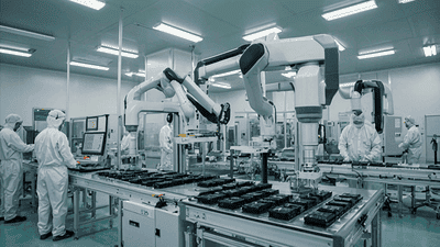
Global Semiconductor Output to Cross $1 Trillion in 2026: Morgan Stanley and SEMI Data
The trillion-dollar semiconductor milestone is no longer merely a forecast. On October 5, 2026, the Semiconductor Industry Association reported that global chip sales had already exceeded $1 trillion through August. August sales reached $159.7 billion, and the association said full-year sales were projected to exceed $1.6 trillion. These are dollar-denominated sales figures—not a measure of physical chip output.
Storage
HBM’s Crowding-Out Effect on DDR4 Supply: The Legacy Memory Shortage
The memory market has developed an uncomfortable contradiction: the technology manufacturers are eager to leave behind can become the product customers struggle hardest to replace. DDR4 is no longer the preferred destination for much of the industry’s new investment, yet a substantial installed base still depends on it.
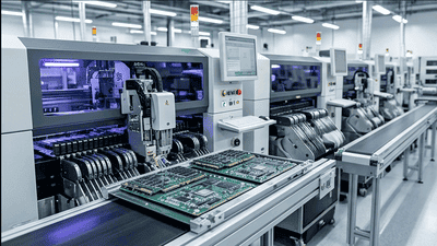
CXL Memory Module Commercialization: The Next Storage Architecture Shift
A server can run out of memory capacity long before it runs out of processing capability. Another can carry expensive DRAM that its applications rarely use. Both situations expose the same architectural limitation: memory has traditionally been purchased, installed, and managed closely around individual processors and systems.

NAND Flash Price Trajectory in 2026: Why Enterprise SSDs Outperform Consumer
The NAND market in 2026 is not following one uniform recovery curve. Enterprise storage is benefiting from expanding data-center requirements, while consumer storage faces a different purchasing environment: higher component costs, more cautious procurement, and greater resistance to passing those costs through to end users.
Equipment
CMP Consumables Business Model: The Recurring Revenue Advantage
Chemical mechanical planarization has an attractive commercial characteristic: the equipment is purchased periodically, but the materials that make it productive are consumed repeatedly. Every qualified polishing process creates continuing demand for slurry, pads, conditioners, cleaning chemistry, and other supporting products.
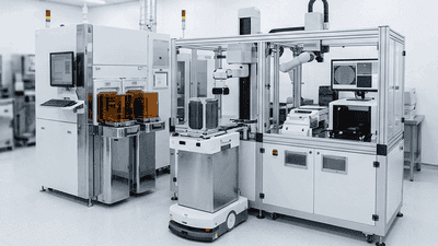
Inspection and Metrology Tools: The Yield Improvement Lever in 3nm
A 3nm manufacturing process can be technically impressive and commercially disappointing at the same time. The difference often lies in how consistently it produces usable devices. Expensive production equipment establishes the capability to manufacture advanced structures; inspection and metrology help determine whether that capability becomes repeatable, economical output.
Ion Implanter Market: China’s Breakthrough Attempts in a Duopoly
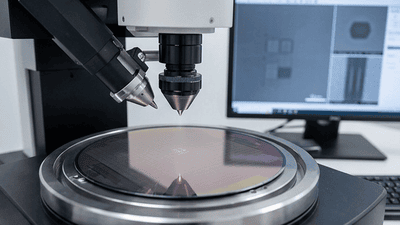
Ion implantation is one of semiconductor manufacturing’s least visible but most consequential processes. The equipment does not attract the attention of extreme ultraviolet lithography, yet it helps determine the electrical properties that make a semiconductor device useful. A carefully controlled ion beam introduces selected species into a wafer, creating a material profile that must work with the rest of the manufacturing process.
Bonder and Molder Demand from CoWoS and HBM: The Back-End Equipment Surge
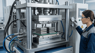
The semiconductor investment cycle is no longer defined only by how many wafers a fab can process. For AI systems, manufacturing capacity also depends on how effectively advanced dies and memory stacks can be assembled into working packages. A wafer full of functioning chips creates limited commercial value if bonding, encapsulation, inspection, or testing cannot keep pace.
Advanced Packaging

The Three-Headed Race in Advanced Packaging: TSMC, Intel, and ASE
For years, chip conversations revolved around transistor nodes and wafer fabs. Today, the more interesting battles are often happening a few millimeters above the silicon, in the world of advanced packaging. As AI, high‑performance computing, and high‑bandwidth memory redefine what a “chip” looks like, three names stand out in the packaging race: TSMC, Intel, and ASE. Each comes from a different starting point, with different strengths and weaknesses, and together they’re reshaping how heterogeneous integration will be done for the next decade.
Competitive Landscape of Advanced Packaging: The Coopetition Between OSATs and Foundries
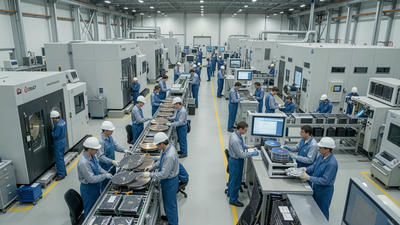
Advanced packaging has moved from the back end of semiconductor manufacturing to the center of the industry’s strategic map. As AI, high-performance computing, mobile systems, automotive electronics, and chiplets all push toward heterogeneous integration, one question has become unavoidable: who owns the packaging layer of the future, OSATs or foundries? The answer is not a clean winner-takes-all outcome. It is a complex and evolving contest of overlap, specialization, and cooperation. In other words, it is cooptition.
New Standards for Cleanroom Grades and Environmental Requirements in Advanced Packaging
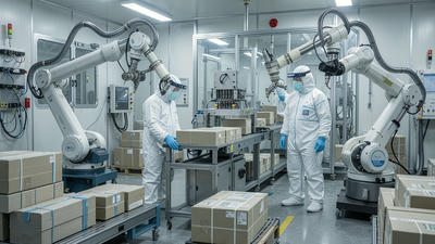
Advanced packaging has changed the rules of semiconductor manufacturing, and cleanroom standards are changing with it. What used to be a largely front-end concern is now a packaging concern too, because heterogeneous integration depends on much more than just transistor quality. It depends on the cleanliness of bonding surfaces, the stability of thin wafers, the behavior of mold compounds, the integrity of fine-pitch interconnects, and the control of particles, humidity, and temperature throughout assembly. In short, the environment has become part of the design.
Materials

Indices
STOXX Europe Semi vs. US Semi: The Long-Term Return Attribution
Europe builds some of the semiconductor industry’s most difficult-to-replace technology. US-listed semiconductor companies include businesses that capture substantial value from chip architecture, computing platforms, and manufacturing equipment. Both belong to the same global production system, yet their equity benchmarks can follow very different paths.

Equal-Weight vs. Cap-Weighted Semi Indices: The Performance Gap
Two semiconductor indices can own the same companies and tell different stories about the industry. One may suggest that chips are enjoying a powerful rally. The other may show that the typical constituent is barely participating. The difference is not necessarily bad data or conflicting forecasts. It can be the weighting method.

Semi Industry Earnings Contribution to S&P 500: The 12% Milestone
When semiconductors approach a double-digit share of a broad equity benchmark’s earnings, the conversation changes. Chips are no longer merely a specialist sector watched by technology analysts. They become a meaningful influence on the profit outlook of the wider market—and, indirectly, on portfolios whose owners may never have deliberately bought a semiconductor fund.
HBM Memory
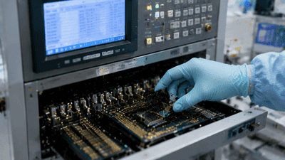
Incremental Demand for HBM Test and Burn-in Equipment – A Quantified Forecast
As High-Bandwidth Memory (HBM) moves from niche to mainstream across AI, HPC, and advanced graphics, test and burn-in equipment emerges as a critical bottleneck. HBM modules require more extensive, higher-fidelity testing than commodity DRAM: multi-die functional tests, high-speed channel validation, thermal stress profiles, and system-level burn-in under representative accelerator loads.

HBM’s Value Share Per AI Server Unit Continues to Rise
High-Bandwidth Memory (HBM) has steadily transitioned from a niche premium to a core system-level enabler for modern AI servers. As models grow larger and throughput demands intensify, designers increasingly attach value to bandwidth, density, and energy efficiency that HBM uniquely provides.

HBM4 Mass Production Kickoff: The 2026 Tech Roadmap Showdown Among 3 Memory Giants
By 2026, high bandwidth memory (HBM) has moved from a niche enabler of premium accelerators to a central battleground in the AI and advanced computing industry. The kickoff of HBM4 mass production marks a decisive escalation: the three leading memory giants are no longer just supplying components; they are effectively shaping the performance envelope and cost structure of the next generation of AI chips.
ETFs
DRAM ETF PCF Changes: The Sentiment Signal
Semiconductor ETFs are often viewed as simple vehicles for gaining diversified exposure to the chip industry. Yet beneath the familiar ETF price chart is a detailed portfolio construction process that can reveal useful information about market expectations. One particularly interesting source of information is the portfolio composition file, commonly referred to as the PCF. Changes in the PCF can show how an ETF's underlying basket is being adjusted, and for DRAM-related semiconductor strategies, these adjustments may provide an early indication of changing investor sentiment.
Thematic Semi ETF Launches in 2026: The Product Innovation Wave
The semiconductor ETF market has entered a more creative phase in 2026. For years, investors could choose from relatively familiar products: broad semiconductor funds, regional technology ETFs, equipment-focused strategies, leveraged products, and a handful of thematic portfolios. The latest wave is different. ETF providers are increasingly attempting to package specific semiconductor narratives into investable products, responding to the growing diversity of the chip industry and to investors who want exposure to individual structural themes rather than the semiconductor sector as a whole.

ETF Flow vs. Korea Export Data: The Lead-Lag Relationship
Semiconductor ETFs have become an increasingly important way for investors to express views on the global chip cycle. Domestic funds, overseas semiconductor ETFs, and leveraged products all provide different forms of exposure, but their movements are often connected to the same underlying economic forces. Among the most useful external indicators for understanding that cycle is South Korea's export data, particularly semiconductor exports.

Semi ETF Tracking Error: The Replication Quality Ranking
Semiconductor ETFs are often marketed around their themes, index exposure, holdings, and historical performance. Yet one of the most important characteristics of an ETF can be much less visible: how accurately the fund actually follows its benchmark. For investors comparing domestic semiconductor ETFs, overseas semiconductor products, and leveraged funds, tracking error provides a practical way to evaluate replication quality.
Compute Chips
Nvidia Rubin’s 288GB HBM4 Configuration: Memory Bandwidth as the New Compute Bottleneck
An AI accelerator can contain extraordinary arithmetic capability and still spend valuable time waiting for data. That gap between what a processor can calculate and what its memory system can supply is central to Nvidia’s Rubin architecture.

Chiplet Design Wins in AI Accelerators: The D2D Interconnect Standard Battle
The next AI accelerator does not necessarily need to be one enormous piece of silicon. It can combine compute tiles, an I/O die, memory interfaces, and specialized engines within a single package. That opens architectural possibilities—but creates a new problem: the pieces must communicate without consuming the performance and efficiency they were assembled to deliver.
Edge NPU Adoption in AI Phones and PCs: 40% Penetration Milestone Reached
AI acceleration is moving from a premium feature toward an ordinary part of personal computing. More phones and PCs now include hardware designed to run neural-network workloads locally, giving manufacturers another way to improve responsiveness, manage power, and introduce software features.