
Materials
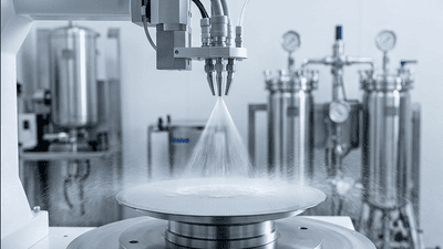
Electronic Grade NaOH: The Cleaning Process Purity Upgrade
In semiconductor materials, the most valuable upgrade is not always a new molecule. Sometimes it is a familiar chemical delivered with tighter impurity limits, cleaner packaging, better analytical verification, and more dependable batch consistency. Electronic-grade sodium hydroxide belongs to that category: a conventional alkaline chemical whose usefulness depends on the application and the contamination controls surrounding it.
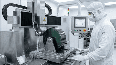
SiC Substrate Cost Curve: Approaching Silicon Parity in 2026
Silicon carbide has moved from an expensive specialist material to a serious contender in high-voltage power electronics. Its performance advantages are well established, but the commercial question has become sharper: how much of the remaining cost premium can manufacturing scale, better yields, and larger wafers remove?
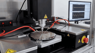
SOI Substrate Demand in RF and Power: The Specialty Wafer Opportunity
A silicon wafer is often described as the foundation of a semiconductor. In silicon-on-insulator technology, that foundation does more than support the manufacturing process. Its engineered structure helps determine how electrical signals behave, how neighboring circuits interact, and how different functions can share a chip.
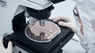
Semiconductor Material Qualification Timeline: 24 to 12 Months
A promising semiconductor material can leave the laboratory long before it earns a place in production. Between those milestones sits qualification: the work of proving that a wafer, photoresist, gas, or sputtering target performs consistently inside a customer’s manufacturing process.
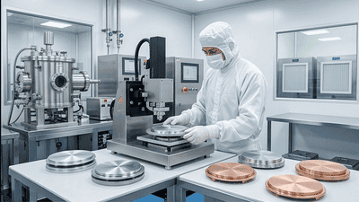
Sputtering Target Material Transition: Al, Cu, Ti, and Co in Advanced Interconnects
The wiring inside a semiconductor is becoming as important to performance as the transistors it connects. As features shrink, moving electrical signals through narrow lines and tiny connections becomes increasingly difficult. Resistance, reliability, and manufacturing consistency turn metallization into a materials-engineering challenge.
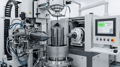
High-Purity Quartz Supply Risk: The Monocrystal Pulling Bottleneck
The semiconductor industry usually describes its vulnerabilities through familiar headlines: lithography restrictions, advanced packaging shortages, scarce photoresists, or interruptions in specialty gases. Yet one of the most consequential dependencies sits much earlier in the manufacturing chain. Before a silicon wafer reaches a fabrication plant, its crystal must be grown. For much of the industry, that means pulling a single crystal from molten silicon held inside a quartz crucible.
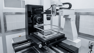
Photomask Localization: Qingyi and Luwei’s Progress
China’s semiconductor localization story is often told through fabrication equipment, silicon wafers, photoresists, and specialty gases. Photomasks receive less attention, despite occupying a decisive position in manufacturing: they carry the patterns that lithography transfers onto a wafer. Without a suitable mask, a qualified process cannot turn a circuit design into repeatable production.
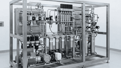
Precursor Demand in ALD and CVD: The Korean Supplier Dominance
A semiconductor’s most important materials are not always visible in the finished device. Some arrive at the factory inside specialized containers, enter a deposition chamber as vapor, and disappear into films only a few nanometers thick. These precursors help form the insulating layers, electrodes, barriers, and other structures that allow modern chips to operate.
Wet Chemicals G5 Purity: The Domestic Qualification Breakthrough
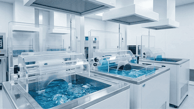
A semiconductor fabrication plant can install advanced equipment, secure high-quality silicon wafers, and develop sophisticated process recipes, yet still lose performance to contamination carried by an ordinary-looking liquid. Sulfuric acid, hydrogen peroxide, hydrofluoric acid, and ammonia solutions appear unremarkable beside a lithography scanner. Inside the fab, however, their cleanliness can influence whether a carefully engineered surface survives the next manufacturing step.
CMP Slurry Advances: Dinglong’s Cerium Oxide and TSV Polishing Wins
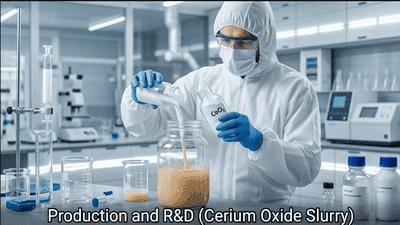
The semiconductor supply chain has a habit of hiding its most consequential dependencies behind its least glamorous materials. Advanced lithography attracts headlines. AI accelerators attract capital. Yet before a chip can become either a technological breakthrough or a commercial success, it needs a wafer—and most mainstream silicon wafer production depends on growing a single crystal inside a quartz crucible.