
Materials
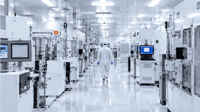
Electronic Specialty Gas Demand from Advanced Nodes: The Localization Acceleration
Semiconductor manufacturing is often described through its most visible assets: lithography machines, cleanrooms, silicon wafers, and increasingly expensive fabrication plants. Yet some of the materials that determine whether those investments produce usable chips arrive through pipes and cylinders. Electronic specialty gases belong to this less visible but strategically important layer of the industry.
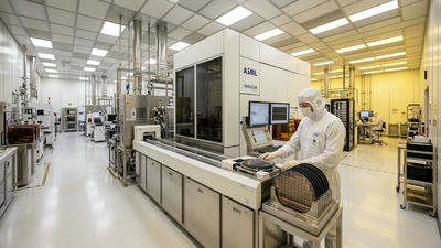
Photoresist Pricing: Shin-Etsu and JSR’s China Strategy Shift
Photoresist pricing has become a revealing lens through which to examine the changing relationship between Japanese materials suppliers and China’s semiconductor industry. For a wafer fab, photoresist is a recurring procurement item. For a process engineer, it is a carefully qualified component of a manufacturing recipe. For a supplier such as Shin-Etsu Chemical or JSR, it represents a combination of chemical expertise, customer integration, and commercial leverage.
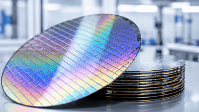
Semiconductor Material Hidden Champions: The Small-Cap Opportunity Map
The semiconductor market rewards visible products: accelerators, memory, leading-edge manufacturing, and the equipment that makes them possible. Far less visible are the materials that allow those operations to run consistently. A wafer, photoresist formulation, specialty gas, or sputtering target may attract little attention until its quality or availability becomes a production problem.
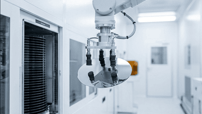
Silicon Wafer Shipment Area Growth: The 2026 Recovery Trajectory
The silicon wafer market is recovering in 2026, but the recovery is neither uniform nor adequately explained by the artificial intelligence investment boom alone. Shipment area is increasing, advanced applications remain the strongest demand engine, and industrial and automotive markets are showing signs of improvement. Yet rising volumes do not automatically imply stronger pricing, fully utilized factories, or an equally healthy outlook across wafer categories.
Wafer Edge Polishing Equipment: The SOI Substrate Demand Driver
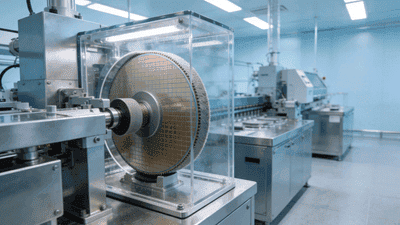
The center of a semiconductor wafer receives most of the attention. That is where engineers measure film thickness, pattern devices, and evaluate electrical performance. The edge looks less productive: a narrow perimeter that cannot accommodate complete dies and often sits outside the usable processing area.
Advanced Packaging Material Demand: Underfill and TIM Localization
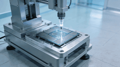
A large AI package can contain exceptional silicon and still fail because a relatively inexpensive material does not behave as expected. An underfill that leaves voids can compromise interconnect reliability. A thermal interface material that loses contact can turn an acceptable cooling design into a temperature problem.
2026 Global Wafer Shipment Area YoY Growth Forecasts: Divergence and Consensus
As the semiconductor industry moves through 2026, expectations for global wafer shipping area growth sit at the core of many strategic decisions. Year‑on‑year (YoY) wafer area forecasts influence how wafer manufacturers plan capacity, how fabs schedule expansions and technology migrations, and how equipment and materials suppliers shape their own production plans. Yet the forecasts themselves are far from uniform. Different institutions—industry bodies, market research firms, banks, and corporate strategists—offer projections that diverge meaningfully in magnitude and composition, even when they point in broadly similar directions.
Shelf Life and Inventory Management of Semi Materials – A Test of Supply Chain Resilience
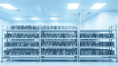
The semiconductor industry is one of the most sophisticated manufacturing ecosystems in the world, relying on thousands of materials with extremely strict quality requirements. From silicon wafers and photoresists to specialty gases, electronic chemicals, and packaging materials, every component must meet precise specifications to ensure stable semiconductor production.
Rising LTA Coverage of Wafer Giants – A Stabilizer for Industry Profitability
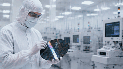
In the complex and cyclical world of semiconductors, stability is a scarce resource. Demand for chips fluctuates with consumer trends, enterprise investments, and macroeconomic swings, while supply chains stretch across continents and multiple tiers of specialized suppliers. Amid this volatility, one segment has become a quiet anchor for industry profitability: the long-term agreements (LTAs) signed between major wafer suppliers and their customers. As LTA coverage rises among wafer giants, it increasingly acts as a stabilizer, smoothing financial performance for both wafer makers and fab operators and reshaping how risk and reward are shared across the value chain.
Qualification Cycles for Domestic Semi Materials Shorten from 24 to 12 Months
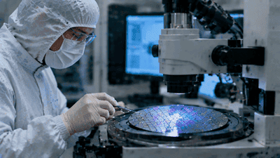
In semiconductor manufacturing, material qualification has traditionally been a long and cautious process. For many critical inputs—wafers, gases, wet chemicals, photoresists, CMP consumables, packaging substrates—domestic suppliers often faced qualification cycles of 18–24 months or more before their products could be used in high‑volume lines. Now, in multiple regions, those cycles are shortening, with leading fabs moving toward 12‑month or even sub‑12‑month qualification for carefully selected domestic materials. This shift reflects both greater confidence in local suppliers and strong strategic pressure to accelerate localization without compromising quality or reliability.