
Materials

CMP Pad and Slurry Market Structure: The Moats of DuPont and Cabot
Chemical mechanical planarization (CMP) is one of the most critical yet often understated processes in semiconductor manufacturing. It quietly ensures that wafers maintain the flat, precisely controlled surfaces needed for successive lithography, etch, and deposition steps. At the center of CMP are two indispensable consumables: pads and slurries. Over the past decades, a small group of global players—most prominently DuPont and Cabot—have built strong positions around these products, developing what can fairly be described as “moats” in the CMP pad and slurry market structure.

The Material System Transition of Sputtering Targets (Al/Cu/Ti/Co) in Advanced Interconnects
Advanced interconnects have quietly become one of the most challenging frontiers in semiconductor manufacturing. As device performance, power efficiency, and reliability demands tighten at each new logic and memory node, the wiring that connects transistors and functional blocks has evolved just as dramatically as the transistors themselves. Central to this evolution is the material system used in thin-film deposition, especially sputtering targets based on aluminum (Al), copper (Cu), titanium (Ti), and cobalt (Co). The transition in these target materials reflects a broader shift in how the industry manages resistance, electromigration, barrier integrity, and manufacturability in increasingly complex interconnect stacks.

Impact of Germanium/Gallium Export Controls on Semi Material Supply Chains
The semiconductor industry has entered a new era in which material security has become as important as technological innovation. For decades, the global chip industry focused primarily on advancing transistor performance, increasing manufacturing efficiency, and expanding semiconductor capacity. However, recent supply chain disruptions and geopolitical tensions have highlighted a critical reality: access to specialized materials can determine the stability and competitiveness of the entire semiconductor ecosystem.

New Application Scenarios of Silicon-Based Materials in 3rd-Gen Semi Substrates
Third-generation semiconductor substrates such as silicon carbide (SiC) and gallium nitride (GaN) are reshaping power electronics, RF devices, and high‑efficiency energy systems. They are often described as a break from traditional silicon, yet silicon‑based materials have not disappeared from the picture. Instead, they have found new, strategically important roles around these wide‑bandgap substrates: as templates, integration platforms, thermal and mechanical partners, and key elements in hybrid packaging. The interplay between silicon and third‑generation semiconductors is becoming a central theme in how next‑generation devices are designed and manufactured.
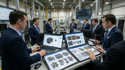
Empirical Analysis of Price Transmission from Material to Foundry End
The semiconductor industry is built upon one of the most complex and interconnected supply chains in the global manufacturing economy. From raw materials and specialty chemicals to semiconductor equipment, wafer fabrication, packaging, and final electronic products, each stage influences the economics of the entire value chain. Among these relationships, the transmission of price changes from semiconductor materials to foundry manufacturing costs has become an increasingly important topic as the industry experiences supply shortages, capacity expansions, and technology transitions.

2026 Photoresist Localization Target of 20%: Which Companies Benefit Most?
The semiconductor industry is entering a period of accelerated transformation as countries and companies increasingly focus on supply chain security, technological independence, and domestic manufacturing capabilities. Among the many semiconductor materials requiring localization, photoresists have become one of the most strategically important categories due to their direct impact on lithography performance, wafer yield, and advanced semiconductor production.
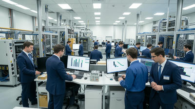
Materials Segment’s Elasticity Coefficient Far Exceeds Design Segment in Upswing
When the semiconductor industry enters an upswing, not all segments respond in the same way. Revenue and profit growth in chip design, manufacturing, equipment, and materials move at different speeds and magnitudes. One of the most striking patterns observed across cycles is how strongly materials segments react compared with the design segment: their “elasticity coefficient” with respect to industry upturns often far exceeds that of design. Put simply, when the cycle turns up, materials businesses frequently grow faster and more sharply than fabless design houses, even though both benefit from rising demand.
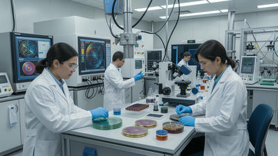
The Price Spread and Capacity Bottlenecks Between EUV and ArF Photoresists
The semiconductor industry has entered an era where advanced manufacturing is no longer limited only by transistor design, lithography machines, or wafer fabrication capacity. Increasingly, the availability, pricing structure, and production scalability of key process materials have become critical factors determining the pace of semiconductor innovation. Among these materials, photoresists occupy a strategically important position because they directly influence the precision, yield, and economic efficiency of semiconductor patterning.

Electronic Specialty Gas Usage Surges in Advanced Nodes, Localization Accelerates
As semiconductor manufacturing pushes deeper into advanced logic and memory nodes, electronic specialty gases have shifted from supporting materials to central enablers of critical processes. Their usage has surged in volume, diversity, and technical importance, particularly in front-end steps such as etch, deposition, doping, and chamber conditioning. At the same time, localization of specialty gas supply—developing domestic or regional production capabilities rather than relying heavily on global imports—has accelerated across multiple semiconductor hubs.
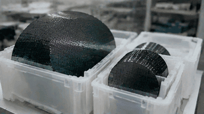
Wafer Size Battle: 300mm Demand Share Continues to Rise, 200mm Stabilizes
The semiconductor industry has always been defined by continuous technological advancement, and wafer size evolution remains one of the most important drivers of manufacturing efficiency. Over the past two decades, the transition from 200mm wafers to 300mm wafers has reshaped semiconductor production economics by enabling higher output, improved cost efficiency, and greater manufacturing scalability. As global demand for advanced computing, artificial intelligence, automotive electronics, and industrial semiconductors continues to expand, the balance between 300mm and 200mm wafer demand is becoming a critical topic across the semiconductor supply chain.